日本の2.4兆円の賭け:Rapidusの2nmチップ開発とAI計算主権の行方
日本の国策半導体企業Rapidusが2nmトランジスタの試作に成功し、半年で5,500億円超を調達した。量産目標は2027年。日本がAI計算基盤を自国で確保できるかを左右する挑戦。
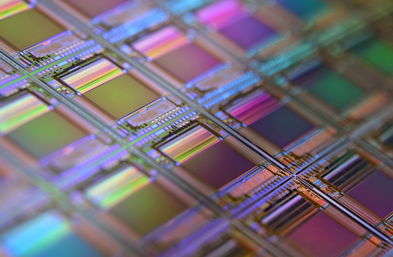
On July 18, 2025, engineers at a foundry in Chitose, Hokkaido, ran current through a 2-nanometer gate-all-around transistor developed with IBM. It showed the electrical characteristics the design called for (Rapidus). Seven months later the company that built it, Rapidus Corporation, founded in 2022, closed a ¥267.6 billion funding round backed by 32 of Japan’s largest companies. Two months after that the government added ¥631.5 billion (TrendForce). By June it had raised another ¥150 billion. Paid-in capital stood at ¥424.95 billion, and METI now puts cumulative government backing at roughly ¥2.4 trillion, around $15–16 billion (Rapidus; TrendForce).
The money is committed. The open questions are the process physics and the customer list, and whether both will be ready by the 2027 date the funding assumes.
Why a foundry
Japan built roughly half the world’s semiconductors in 1988. By the mid-2020s its most advanced domestic logic node was two technology generations behind TSMC and Samsung, both of which reached volume 2-nanometer production in the fourth quarter of 2025, about two years ahead of the Rapidus target (The Register). Rapidus was set up in 2022 to skip the intermediate nodes and go straight to 2nm gate-all-around transistors, working with IBM and Belgium’s imec.
Japanese industrial policy has usually kept some distance from the companies it subsidises. This time the government holds 11.5% of Rapidus’s voting rights plus a “golden share” with veto power over key management decisions (The Register). METI minister Ryosei Akazawa has called it “a national project that must succeed” (The Register) and “a cornerstone of Japan’s crisis management investment plans” (Nikkei Asia).
The timeline so far
Groundbreaking on the IIM-1 fab was September 2023. The cleanroom was complete by 2024. EUV lithography equipment went in that December, and the first EUV exposure ran on April 1, 2025 (Rapidus). The working 2nm GAA transistor followed in July. In April 2026, Rapidus Chiplet Solutions, the company’s back-end packaging arm, also in Chitose, moved from limited operations to full-scale production of a prototype 600mm-square RDL interposer panel, the packaging step that turns a finished die into a usable chip (TrendForce). A process design kit, the toolkit customers need to design chips for the process, was targeted for release in Q1 2026 (Rapidus). Mass production is still targeted for 2027.
Each milestone so far has landed roughly on schedule. First-of-a-kind foundry projects usually slip.
Money ahead of customers
As of the most recent reporting, more than 60 companies are in talks with Rapidus about 2nm capacity. None has signed a volume agreement (JStories). The company’s plan targets an initial run rate of roughly 6,000 wafers per month, scaling toward 25,000 within a year of the mass-production start, at roughly ¥3–3.5 million ($18,500–$21,600) per wafer (JStories). The customers those numbers depend on are still at the design-partnership stage.
Demand is there. TSMC told its largest customers in mid-2026 to expect price increases of 5–10%, and has said its 2nm and 3nm capacity is committed into 2027. AI accelerators have taken the leading-edge supply that used to go to consumer chips, and the shortage has reached retail prices for the iPad, Xbox and Nintendo Switch 2 (JStories). Rapidus is aiming at the demand TSMC cannot physically supply on the AI buildout’s timeline, rather than at TSMC’s existing customers.
Omdia principal analyst Manoj Sukumaran: “I don’t think that Rapidus will be a serious competitor to TSMC all of a sudden.” He pointed to unfinished work on design-tool integration and IP validation before the foundry can reliably deliver customer products, and called getting this far “great progress” from a national-sovereignty standpoint (The Register).
What a domestic foundry buys
A domestic 2nm foundry will not by itself make Japan cost-competitive with TSMC. Rapidus’s own roadmap allows for a multi-year technology gap even if everything goes to plan. What it gives Japan is a supply path that does not run entirely through Taiwan, at a time when the rest of Japan’s AI strategy assumes domestic and allied firms can get leading-edge silicon.
The same applies to Japan’s climate-tech and deep-tech plans. Grid-optimisation models, materials discovery for batteries and fusion, climate and disaster-response simulation all run on the compute layer underneath them. A foundry three years from proving volume shipment moves more slowly than the capital and policy stories around it, and investors tracking the software and funding layers tend to pay it less attention than the fab deserves.
What to watch through 2027
Whether the Q1 2026 process design kit turns design partners into paying customers within 2026. Sixty companies talking and sixty companies buying are different states, and the plan depends on the second.
Whether the back-end packaging line’s move from prototype to full-scale production keeps pace with the front-end fab. A 2nm die without advanced packaging capacity is an unfinished product.
Whether the 2027 mass-production date survives one more funding round. Foundry projects in this category have each hit at least one schedule revision; Rapidus has not yet had to absorb one.
Rapidus is not a sure thing. It is the physical-infrastructure story under every other Japan-AI headline, and the one that will set the limit if the software side outruns supply.
Tech for Impact Summit 2027 runs 18–19 May 2027 in Tokyo, invitation-only. The compute layer sits under every conversation the summit holds on AI, climate and deep tech in Japan, and its Strategy Dialogue format puts the people building, financing and regulating it at one table. You can join the waitlist to be considered for an invitation.